- 您现在的位置:买卖IC网 > Sheet目录2006 > LTC2498IUHF#TRPBF (Linear Technology)IC ADC 24BIT 16CH 38-QFN
LTC2498
30
2498ff
applications inForMation
The LTC6078 is an excellent amplifier for this function. It
operates with supply voltages as low as 2.7V and its noise
level is 18nV/√Hz. The Easy Drive input technology of the
LTC2498 enables an RC network to be added directly to
the output of the LTC6078. The capacitor reduces the
magnitude of the current spikes seen at the input to the
ADC and the resistor isolates the capacitor load from the
op-amp output enabling stable operation.
Reference Current
Similar to the analog inputs, the LTC2498 samples the
differential reference pins (REF+ and REF–) transferring
small amounts of charge to and from these pins, thus
producing a dynamic reference current. If incomplete set-
tling occurs (as a function the reference source resistance
andreferencebypasscapacitance)linearityandgainerrors
are introduced.
For relatively small values of external reference capaci-
tance (CREF < 1nF), the voltage on the sampling capacitor
settles for reference impedances of many k (if CREF =
100pF up to 10k will not degrade the performance), see
Figures 14, 15.
In cases where large bypass capacitors are required on
the reference inputs (CREF > 0.01F) full-scale and linear-
ity errors are proportional to the value of the reference
resistance. Every ohm of reference resistance produces
a full-scale error of approximately 0.5ppm (while operat-
ing in simultaneous 50Hz/60Hz mode), see Figures 16
and 17. If the input common mode voltage is equal to
the reference common mode voltage, a linearity error of
approximately 0.67ppm per 100 of reference resistance
results, see Figure 18. In applications where the input and
reference common mode voltages are different, the errors
increase. A 1V difference in between common mode input
andcommonmodereferenceresultsina6.7ppmINLerror
for every 100 of reference resistance.
In addition to the reference sampling charge, the reference
ESDprojectiondiodeshaveatemperaturedependentleak-
age current. This leakage current, nominally 1nA (±10nA
max) results in a small gain error. A 100 reference
resistance will create a 0.5V full scale error.
Normal Mode Rejection and Anti-Aliasing
One of the advantages delta-sigma ADCs offer over
conventional ADCs is on-chip digital filtering. Combined
with a large oversample ratio, the LTC2498 significantly
simplifies anti-aliasing filter requirements. Additionally,
the input current cancellation feature allows external
lowpass filtering without degrading the DC performance
of the device.
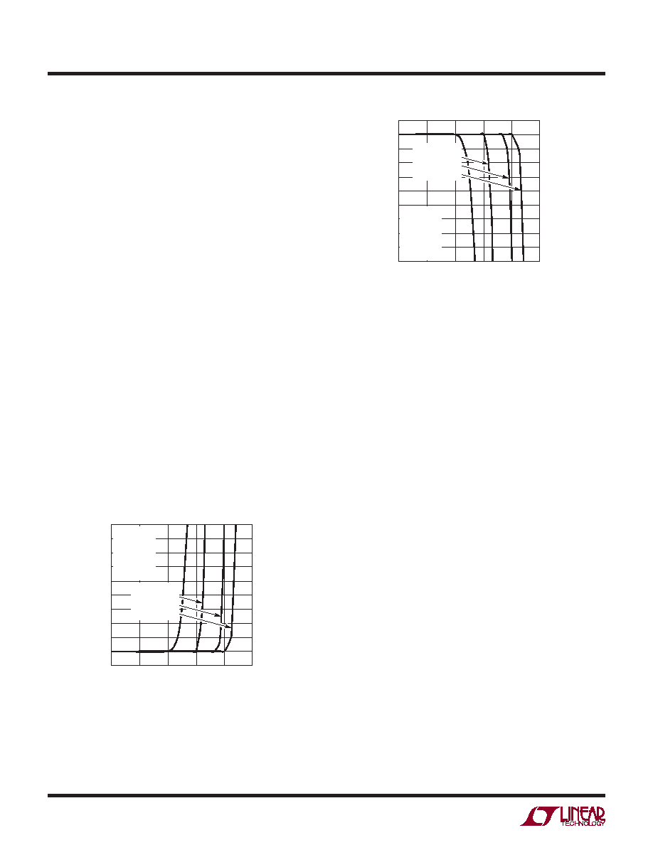
Figure 14. +FS Error vs RSOURCE at VREF (Small CREF)
Figure 15. –FS Error vs RSOURCE at VREF (Small CREF)
RSOURCE ()
0
+FS
ERROR
(ppm)
50
70
90
10k
2498 F14
30
10
40
60
80
20
0
–10
10
100
1k
100k
VCC = 5V
VREF = 5V
VIN+ = 3.75V
VIN– = 1.25V
fO = GND
TA = 25°C
CREF = 0.01F
CREF = 0.001F
CREF = 100pF
CREF = 0pF
RSOURCE ()
0
–FS
ERROR
(ppm) –30
–10
10
10k
2498 F15
–50
–70
–40
–20
0
–60
–80
–90
10
100
1k
100k
VCC = 5V
VREF = 5V
VIN+ = 1.25V
VIN– = 3.75V
fO = GND
TA = 25°C
CREF = 0.01F
CREF = 0.001F
CREF = 100pF
CREF = 0pF
发布紧急采购,3分钟左右您将得到回复。
相关PDF资料
LTC2600IUFD#PBF
IC DAC OCTAL R-R 16BIT 20-QFN
LTC2602IMS8#TRPBF
IC DAC 16BIT DUAL R-R VOUT 8MSOP
LTC2604IGN-1#TRPBF
IC DAC 16BIT QUAD R-R OUT 16SSOP
LTC2605IGN-1#TRPBF
IC DAC 16BIT OCT I2C 16-SSOP
LTC2606IDD#TRPBF
IC DAC 16BIT I2C V-OUT 10-DFN
LTC2607IDE#TRPBF
IC DAC 16BIT R-R I2C 12-DFN
LTC2609CGN#PBF
IC DAC 16BIT R-R QUAD 16SSOP
LTC2621IDD-1#PBF
IC DAC 12BIT R-R 10-DFN
相关代理商/技术参数
LTC2499CUHF
制造商:Linear Technology 功能描述:ADC Single Delta-Sigma 7.5sps 24-bit Serial 38-Pin QFN EP
LTC2499CUHF#PBF
功能描述:IC ADC 24BIT DELTA SIG 38-QFN RoHS:是 类别:集成电路 (IC) >> 数据采集 - 模数转换器 系列:- 标准包装:1 系列:microPOWER™ 位数:8 采样率(每秒):1M 数据接口:串行,SPI? 转换器数目:1 功率耗散(最大):- 电压电源:模拟和数字 工作温度:-40°C ~ 125°C 安装类型:表面贴装 封装/外壳:24-VFQFN 裸露焊盘 供应商设备封装:24-VQFN 裸露焊盘(4x4) 包装:Digi-Reel® 输入数目和类型:8 个单端,单极 产品目录页面:892 (CN2011-ZH PDF) 其它名称:296-25851-6
LTC2499CUHF#TRPBF
功能描述:IC ADC 24BIT DELTA SIG 38-QFN RoHS:是 类别:集成电路 (IC) >> 数据采集 - 模数转换器 系列:- 标准包装:1,000 系列:- 位数:16 采样率(每秒):45k 数据接口:串行 转换器数目:2 功率耗散(最大):315mW 电压电源:模拟和数字 工作温度:0°C ~ 70°C 安装类型:表面贴装 封装/外壳:28-SOIC(0.295",7.50mm 宽) 供应商设备封装:28-SOIC W 包装:带卷 (TR) 输入数目和类型:2 个单端,单极
LTC2499CUHFPBF
制造商:Linear Technology 功能描述:24bit Delta Sigma ADC Temp Sens LTC2499
LTC2499IUHF#PBF
功能描述:IC ADC 24BIT DELTA SIG 38-QFN RoHS:是 类别:集成电路 (IC) >> 数据采集 - 模数转换器 系列:- 标准包装:1 系列:microPOWER™ 位数:8 采样率(每秒):1M 数据接口:串行,SPI? 转换器数目:1 功率耗散(最大):- 电压电源:模拟和数字 工作温度:-40°C ~ 125°C 安装类型:表面贴装 封装/外壳:24-VFQFN 裸露焊盘 供应商设备封装:24-VQFN 裸露焊盘(4x4) 包装:Digi-Reel® 输入数目和类型:8 个单端,单极 产品目录页面:892 (CN2011-ZH PDF) 其它名称:296-25851-6
LTC2499IUHF#TRPBF
功能描述:IC ADC 24BIT DELTA SIG 38-QFN RoHS:是 类别:集成电路 (IC) >> 数据采集 - 模数转换器 系列:- 标准包装:1,000 系列:- 位数:16 采样率(每秒):45k 数据接口:串行 转换器数目:2 功率耗散(最大):315mW 电压电源:模拟和数字 工作温度:0°C ~ 70°C 安装类型:表面贴装 封装/外壳:28-SOIC(0.295",7.50mm 宽) 供应商设备封装:28-SOIC W 包装:带卷 (TR) 输入数目和类型:2 个单端,单极
LTC2600CGN
功能描述:IC DAC OCTAL R-R 16BIT 16SSOP RoHS:否 类别:集成电路 (IC) >> 数据采集 - 数模转换器 系列:- 产品培训模块:Data Converter Fundamentals
DAC Architectures 标准包装:750 系列:- 设置时间:7µs 位数:16 数据接口:并联 转换器数目:1 电压电源:双 ± 功率耗散(最大):100mW 工作温度:0°C ~ 70°C 安装类型:表面贴装 封装/外壳:28-LCC(J 形引线) 供应商设备封装:28-PLCC(11.51x11.51) 包装:带卷 (TR) 输出数目和类型:1 电压,单极;1 电压,双极 采样率(每秒):143k
LTC2600CGN#PBF
功能描述:IC DAC OCTAL R-R 16BIT 16SSOP RoHS:是 类别:集成电路 (IC) >> 数据采集 - 数模转换器 系列:- 产品培训模块:Lead (SnPb) Finish for COTS
Obsolescence Mitigation Program 标准包装:50 系列:- 设置时间:4µs 位数:12 数据接口:串行 转换器数目:2 电压电源:单电源 功率耗散(最大):- 工作温度:-40°C ~ 85°C 安装类型:表面贴装 封装/外壳:8-TSSOP,8-MSOP(0.118",3.00mm 宽) 供应商设备封装:8-uMAX 包装:管件 输出数目和类型:2 电压,单极 采样率(每秒):* 产品目录页面:1398 (CN2011-ZH PDF)